- 您现在的位置:买卖IC网 > Sheet目录488 > NTF3055-160T1 (ON Semiconductor)MOSFET N-CH 60V 2A SOT223
NTF3055-160
Preferred Device
Power MOSFET
2.0 Amps, 60 Volts
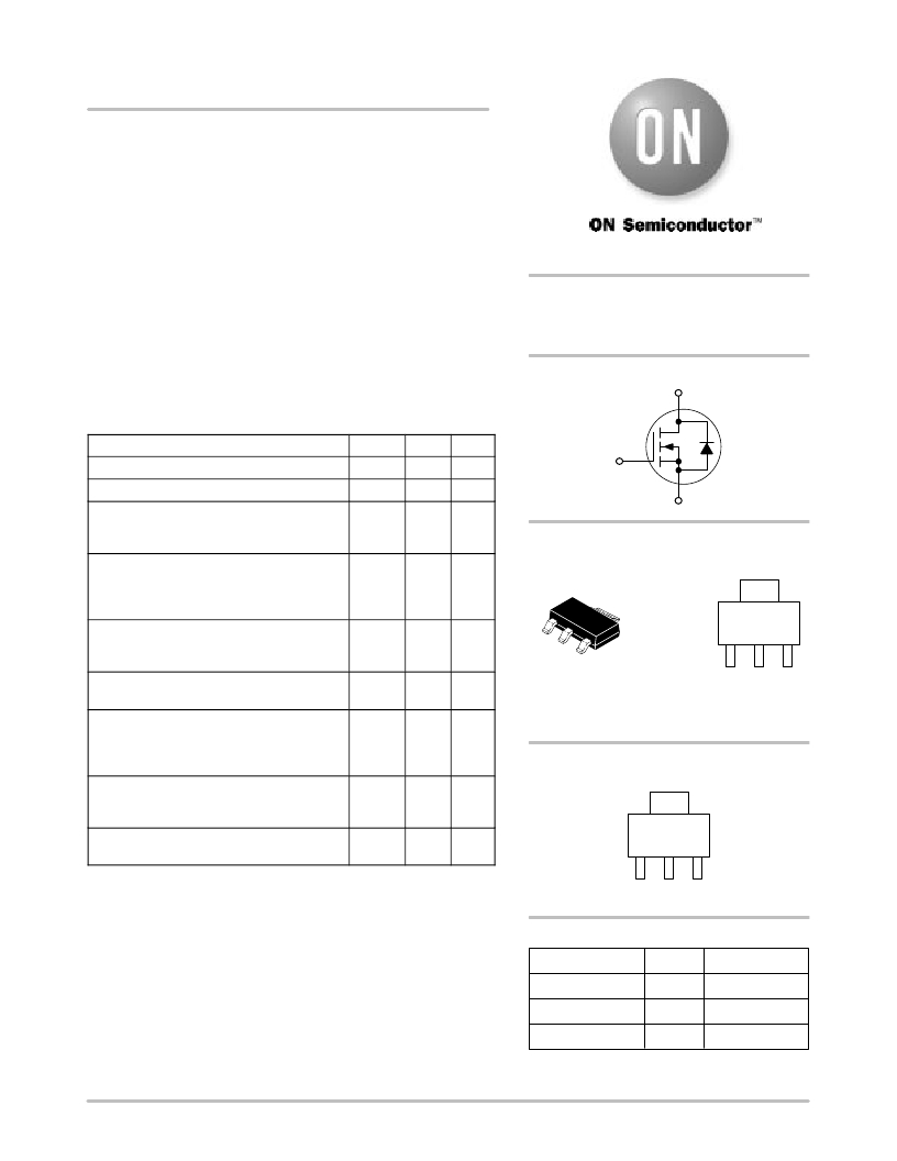
N–Channel SOT–223
Designed for low voltage, high speed switching applications in
power supplies, converters and power motor controls and bridge
circuits.
Applications
http://onsemi.com
2.0 AMPERES
?
?
?
?
Power Supplies
Converters
Power Motor Controls
Bridge Circuits
60 VOLTS
RDS(on) = 160 m W
N–Channel
D
MAXIMUM RATINGS (TC = 25 ° C unless otherwise noted)
Rating
Symbol
Value
Unit
Drain–to–Source Voltage
VDSS
60
Vdc
G
Drain–to–Gate Voltage (RGS = 1.0 M ? )
Gate–to–Source Voltage
– Continuous
– Non–repetitive (tp ≤ 10 ms)
VDGR
VGS
60
± 20
± 30
Vdc
Vdc
Vpk
S
MARKING
Drain Current
DIAGRAM
– Continuous @ TA = 25 ° C
– Continuous @ TA = 100 ° C
– Single Pulse (tp ≤ 10 μ s)
Total Power Dissipation @ TA = 25 ° C (Note 1.)
Total Power Dissipation @ TA = 25 ° C (Note 2.)
Derate above 25 ° C
ID
ID
IDM
PD
2.0
1.2
6.0
2.1
1.3
0.014
Adc
Apk
W
W
W/ ° C
1
2
3
4
SOT–223
CASE 318E
STYLE 3
5160
LWW
Operating and Storage Temperature Range
TJ, Tstg
–55 to
175
° C
5160
= Device Code
L
= Location Code
Single Pulse Drain–to–Source Avalanche
Energy – Starting TJ = 25 ° C
EAS
65
mJ
WW
= Work Week
(VDD = 25 Vdc, VGS = 10 Vdc,
IL(pk) = 6.0 Apk, L = 10 mH, VDS = 60 Vdc)
PIN ASSIGNMENT
Thermal Resistance
° C/W
4 Drain
– Junction to Ambient (Note 1.)
– Junction to Ambient (Note 2.)
R θ JA
R θ JA
72.3
114
Maximum Lead Temperature for Soldering
Purposes, 1/8 ″ from case for 10 seconds
TL
260
° C
1. When surface mounted to an FR4 board using 1 ″ pad size,
(Cu. Area 1.127 in2).
2. When surface mounted to an FR4 board using minimum recommended pad
1
Gate
2
Drain
3
Source
size, 2–2.4 oz. (Cu. Area 0.272 in2).
ORDERING INFORMATION
Device
Package
Shipping
NTF3055–160T1
NTF3055–160T3
NTF3055–160T3LF
SOT–223 1000 Tape & Reel
SOT–223 4000 Tape & Reel
SOT–223 4000 Tape & Reel
? Semiconductor Components Industries, LLC, 2001
July, 2001 – Rev. 0
1
Publication Order Number:
NTF3055–160/D
发布紧急采购,3分钟左右您将得到回复。
相关PDF资料
NTF3055L108T3LFG
MOSFET N-CH 60V 3A SOT223
NTF3055L175T1
MOSFET N-CH 60V 2A SOT223
NTF5P03T3G
MOSFET P-CH 30V 3.7A SOT223
NTF6P02T3G
MOSFET PWR P-CHAN 10A 20V SOT223
NTGD3133PT1G
MOSFET P-CH DUAL 20V 21.5A 6TSOP
NTGD3147FT1G
MOSFET P-CH 20V 2.2A 6-TSOP
NTGD3148NT1G
MOSFET N-CH DUAL 20V 3.5A 6TSOP
NTGD3149CT1G
MOSFET COMPL 20V DUAL 6-TSOP
相关代理商/技术参数
NTF3055-160T3
制造商:Rochester Electronics LLC 功能描述:- Bulk
NTF3055-160T3LF
功能描述:MOSFET N-CH 60V 2A SOT223 RoHS:否 类别:分离式半导体产品 >> FET - 单 系列:- 标准包装:1,000 系列:MESH OVERLAY™ FET 型:MOSFET N 通道,金属氧化物 FET 特点:逻辑电平门 漏极至源极电压(Vdss):200V 电流 - 连续漏极(Id) @ 25° C:18A 开态Rds(最大)@ Id, Vgs @ 25° C:180 毫欧 @ 9A,10V Id 时的 Vgs(th)(最大):4V @ 250µA 闸电荷(Qg) @ Vgs:72nC @ 10V 输入电容 (Ciss) @ Vds:1560pF @ 25V 功率 - 最大:40W 安装类型:通孔 封装/外壳:TO-220-3 整包 供应商设备封装:TO-220FP 包装:管件
NTF3055L108
制造商:ONSEMI 制造商全称:ON Semiconductor 功能描述:Power MOSFET 3.0 A, 60 V, Logic Level, N−Channel SOT−223
NTF3055L108/D
制造商:未知厂家 制造商全称:未知厂家 功能描述:Power MOSFET 3.0 Amps, 60 Volts, Logic Level
NTF3055L108D
制造商:ONSEMI 制造商全称:ON Semiconductor 功能描述:Power MOSFET 3.0 A, 60 V, Logic Level, N−Channel SOT−223
NTF3055L108T1
功能描述:MOSFET 60V 3A N-Channel RoHS:否 制造商:STMicroelectronics 晶体管极性:N-Channel 汲极/源极击穿电压:650 V 闸/源击穿电压:25 V 漏极连续电流:130 A 电阻汲极/源极 RDS(导通):0.014 Ohms 配置:Single 最大工作温度: 安装风格:Through Hole 封装 / 箱体:Max247 封装:Tube
NTF3055L108T1G
功能描述:MOSFET 60V 3A N-Channel RoHS:否 制造商:STMicroelectronics 晶体管极性:N-Channel 汲极/源极击穿电压:650 V 闸/源击穿电压:25 V 漏极连续电流:130 A 电阻汲极/源极 RDS(导通):0.014 Ohms 配置:Single 最大工作温度: 安装风格:Through Hole 封装 / 箱体:Max247 封装:Tube
NTF3055L108T3
功能描述:MOSFET 60V 3A N-Channel RoHS:否 制造商:STMicroelectronics 晶体管极性:N-Channel 汲极/源极击穿电压:650 V 闸/源击穿电压:25 V 漏极连续电流:130 A 电阻汲极/源极 RDS(导通):0.014 Ohms 配置:Single 最大工作温度: 安装风格:Through Hole 封装 / 箱体:Max247 封装:Tube
